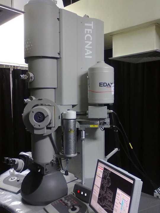
Technical Specification
|
| Electron Source |
FEG Source |
| Operating Voltages |
200kV, 120kV, 80kV |
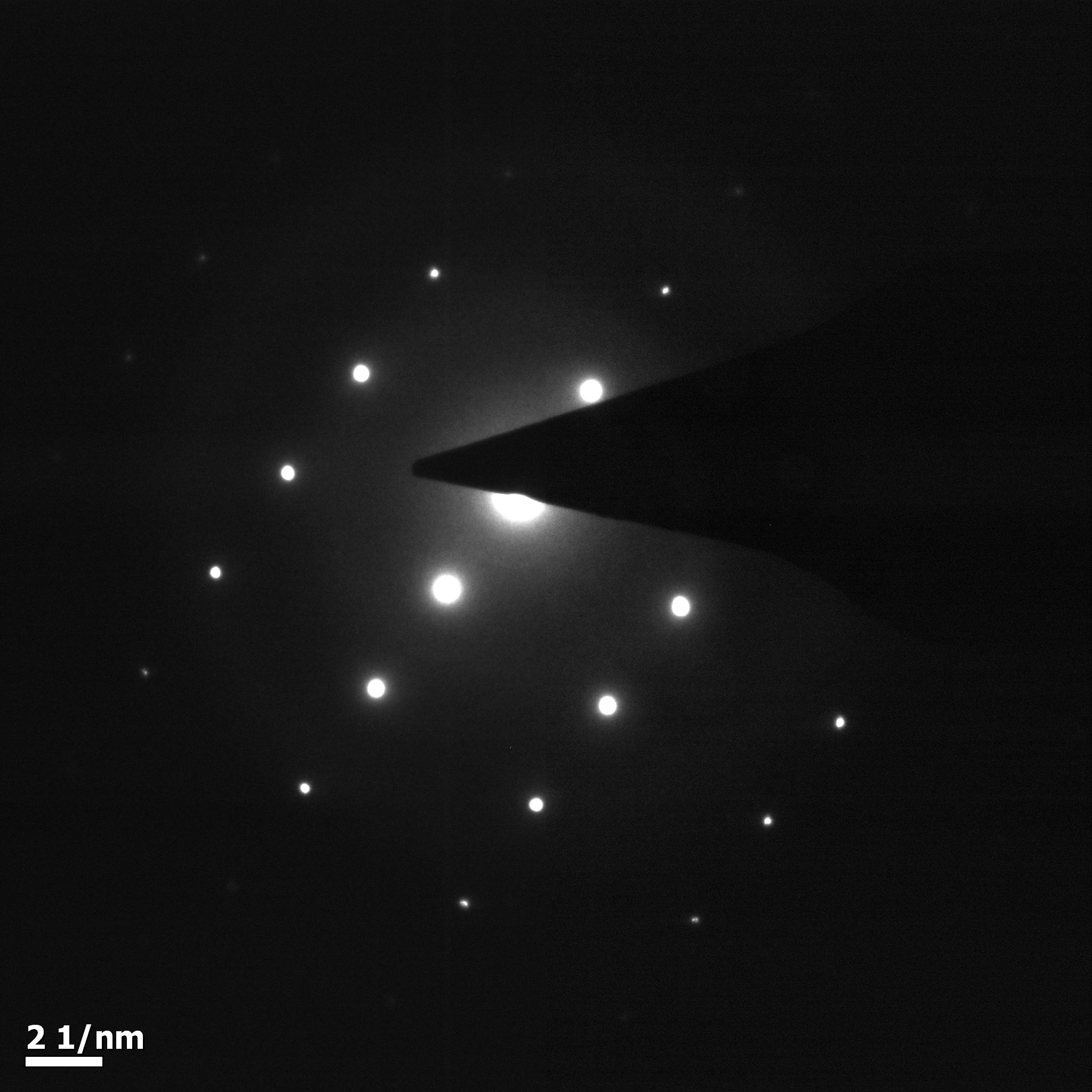
| Imaging Modes: |
- Bright field (BF)
- Dark Field (DF)
- High Resolution Imaging (HRTEM)
- Selective Area Diffraction Pattern (SAD)
- S-TEM Imaging
|
| Analysis Mode |
EDS Analysis
STEM-EDS Mapping (Point/Line /Area Mapping) |
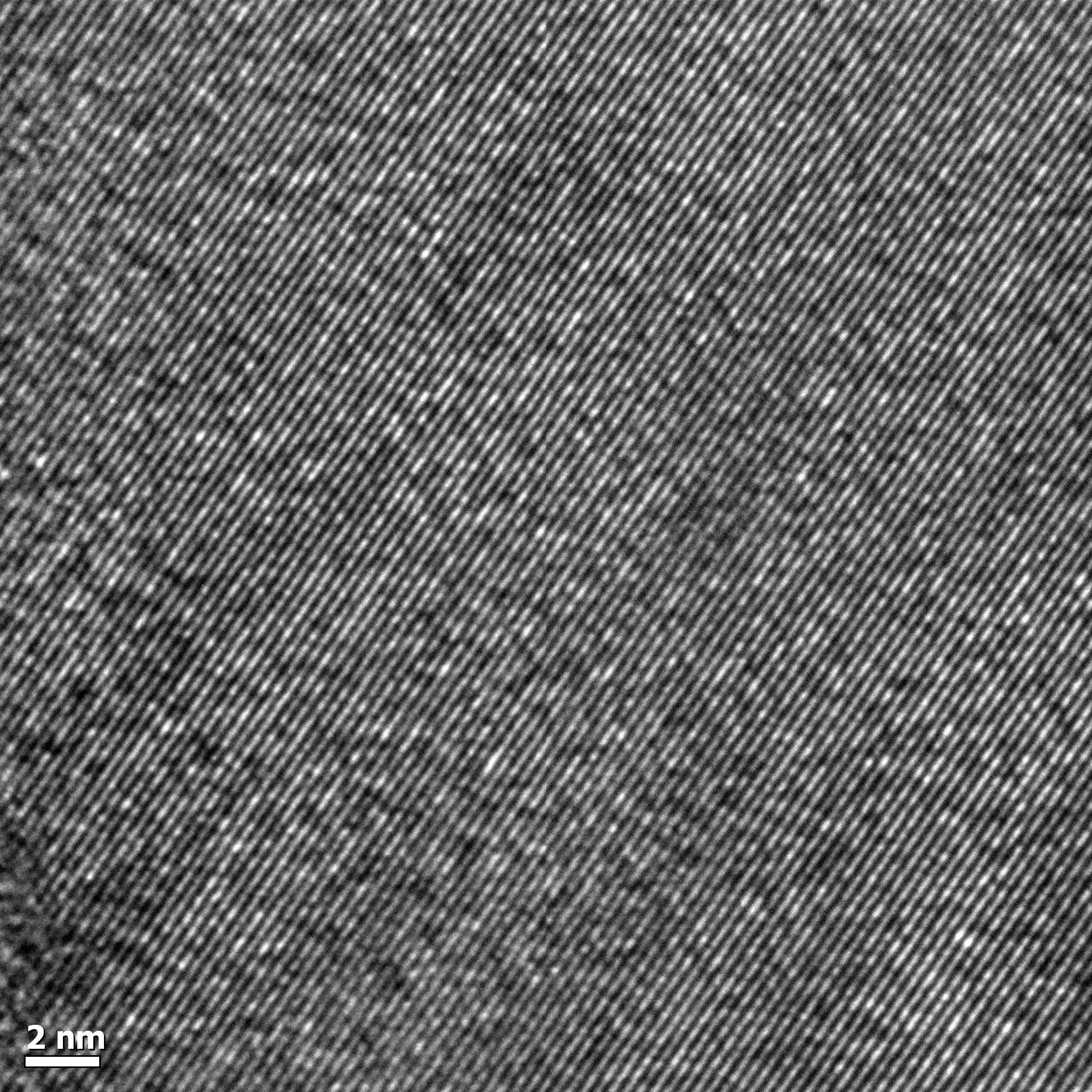
| Resolution |
| TEM point resolution (nm) |
0.24 |
| TEM line resolution (nm) |
0.102 |
| STEM resolution (nm) |
0.19 |
|
Detectors
|
- Bottom mount CCD detector for TEM, HRTEM imaging
- EDAX Detector for EDS Analysis in TEM, STEM mode.
- High Angle Annular Dark Field Detector for STEM imaging.
|
HRTEM up-gradation
|
| With the existing HRTEM in 2012 Gatan Imaging Filter (GIF) Detector has been attached which is capable of doing Chemical analysis of the TEM sample. |
GIF Specification
|
| Operation Modes |
- Energy Filter TEM Imaging (EFTEM)
- Electron Energy Loss Spectrometry(EELS)
- TEM-EELS
- STEM-EELS (Point/Line/Area Mapping)
|
| Operating Voltages |
200kV, 120kV |
| Energy Field of view (eV) |
2000 |
| Resolution |
| Energy Resolution (eV FWHM) |
0.25 |
|
Detector
|
| Energy Filter CCD detector for EFTEM Imaging and EELS Spectrometry |